- DLA/DSCC Certified Products
- QML/SMD 5962
- Function
- MIL-STD-1553
- Memory
- Logic Devices
- Analog
- Nuclear Event Detector (NED)
- Advanced Interconnect Technologies
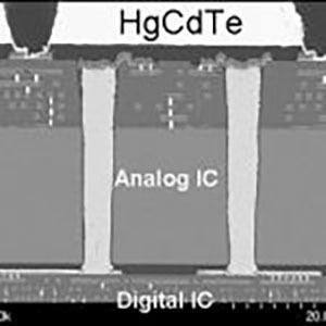
- 2.5 & 3D Heterogeneous Integration
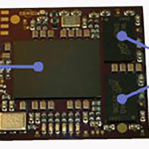
- System in Package (SiP)
- Wafer Bumping & WLP
- Multi-Chip Modules (MCMs)
- Novel Microfabrication & MEMS
- Design, Packaging & Assembly
- Assembly Services
- Final Test
- Chip on Board (CoB)
- Plastic Packaging (BGA/CSP/QFN)
- Hermetic Packaging
- MIL-STD-1553 Data Bus Couplers & Accessories
- Micro In-Line Couplers
- Tab Mounted In-Line Couplers
- Through Hole Mounted In-Line Couplers
- Box Couplers
- Custom Design Couplers
- Data Bus Coupling Transformers
- Data Bus Relays
- Data Bus Harnesses
- Bus and Stub Terminators
- Wide Bandwidth RF & Video Transformers
- Antenna Couplers
- Video Isolation Transformers
- RF Wideband Transformers
- RF Wideband Transformers & Impedance Adapters
Micross AIT works with a wide variety of clients and partners, bringing integrated process, design, testing and analysis capabilities to projects involving custom application-driven development.
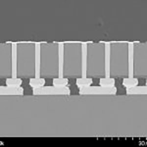
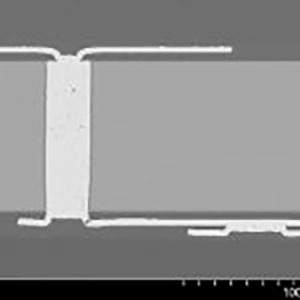
Micross AIT offers access to our 2.5D/3D technology platform through joint development projects, prototyping services and small volume production. Our 2.5D/3D integration technology platform is based on several enabling process modules, which include:
- Through-silicon via (TSV) interconnects
- High density 3D IC applications, filled 2-10 μm diameter, up to 8:1 aspect ratio and 10-50 μm pitch
- Lower density 2.5D/3D package architectures, 10-50 μm diameter, aspect ratio of 4:1 to 6:1 and 50-500 μm pitch; vias can be filled or barrel coated
- Wafer thinning (to < 20 μm Si thickness) and processing on temporary carrier wafer
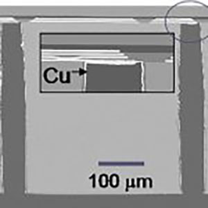
- Flip-chip and high-density metal-metal bonding, down to <10 μm pitch
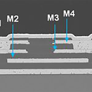
- Large-area multi-level metal routing with standard RDL (down to 10 μm L/S) or dual damascene process (down to 6 μm L/S)