|
The Most Complete Provider of Advanced Microelectronic Services
and Component, Die & Wafer Solutions
|
|
|
|
|
|
September 2025 | 300mm Wafer Processing & Advanced Packaging The semiconductor industry is undergoing a significant transformation as the latest technologies are being produced on 300mm silicon wafers to maximize production efficiency and reduce costs. TSMC, Samsung, Global Foundries, Micron Technologies, and Texas Instruments are investing significantly in 300mm semiconductor foundries across the United States. Meanwhile, in compound semiconductors (GaN, SiC, GaAs), state-of-the-art technologies can vary from 100-200mm depending on materials sets. Micross is setup to be part of your technology solution, with capabilities to process, package, and assemble all wafer diameters and technologies. To learn more, visit www.micross.com, or meet with us at our upcoming tradeshows to discuss your semiconductor requirements!
|
|
|
|
|
|
|
|
|
|
Sourcing Bare Die & Wafer Micross is the largest franchised global supplier of bare die with access to thousands of different devices types and the latest Si and compound material. Offering unparalleled knowledge & extensive capabilities as well as the flexibility to adapt our suppliers’ standard products to the unique requirements of your device or system.
|
|
|
|
|
|
|
|
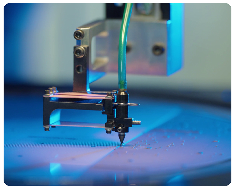
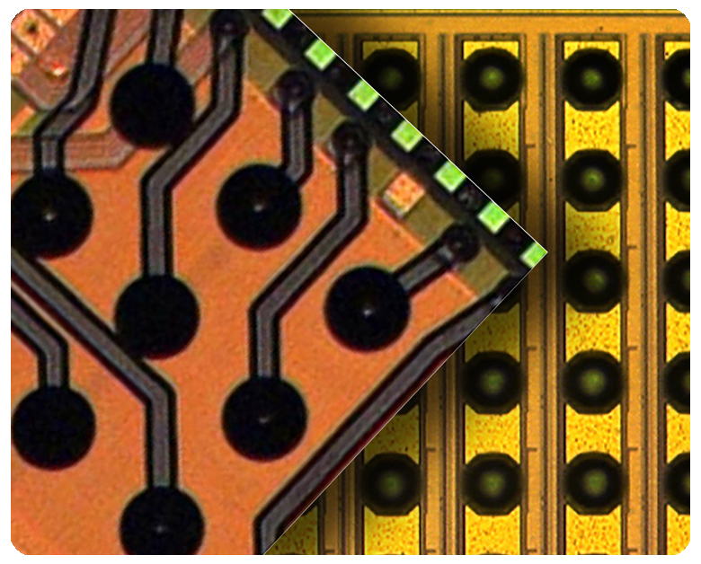
Wafer Processing
Micross is the largest worldwide value-added bare die processor with a comprehensive array of capabilities to fully process wafers from 100mm to 300mm. Whether a commercial product or your own die design, we will process wafer product to your exact specifications and choice of end supply form - Wafer Probe / Mapping
- Wafer Thinning & Finishing
- Wafer Dicing
- Visual Inspection
- Temporary Bonding / De-Bonding
|
|
|
|
|
|
|
|
|
|
Advanced Interconnect Technology (AIT) Micross AIT enables designers to realize optimized multi-chip devices by integrating the latest 300mm Si devices, with State-of-the art foundry technology nodes (GaN, SiC, GaAs) produced on 100mm to 200mm wafers. - 2.5/3D Heterogeneous Chiplet Integration
- Redistribution Layers (RDLs): Fan-In / Fan-Out
- Photonic Interconnects
- Wafer Bumping & Wafer-Level Packaging (WLP)
- Through Silicon Vias (TSV)
- Pb & Pb-Free C4 Bumping & Cu Pillar Bumping
|
|
|
|
|
|
|
|
DoD Contract Expands AIT OSAT Capabilites Our 300mm capabilities will be further augmented as a result of receiving the $130+ million IBAS Cornerstone Re-shore Ecosystem for Secure Heterogeneous Advanced Packaged Electronics (RESHAPE) awarded by the US Department of Defense.
|
|
|
|
|
|
|
|
|
|
EOL Die Sustainment Program (EDSP) As foundries and manufacturers focus their resources on developing new technologies and scaling up 300mm wafer production, older fabrication lines may be deprioritized or even phased out. Micross EDSP provides continuous device availability for products that have or may become end-of-life, enabling the avoidance of costly re-qualification, overhead costs, resource utilization, and production delays. OEMs and Contractors: Fortify your supply chain & ensure a continuous supply of components throughout the entire life-cycle of your program. Micross will provide long-term storage for bare die, wafer, and materials, and will process, package, and test devices as needed. Foundries & Die Suppliers: Micross enables you to refocus product line resources to 300mm production by utilizing our world-class wafer processing and OSAT services to manufacturer your devices, while continuing to offer 100-200mm products to your customers
|
|
|
|
|
|
|
|
|
|
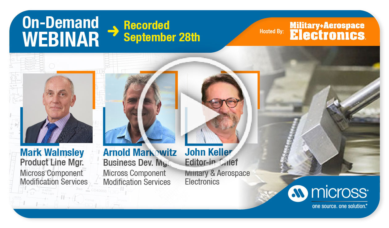
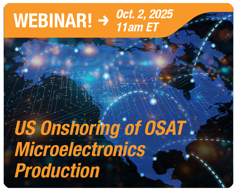
Developing Advanced Packaging Supply Chains for Onshore Microelectronics Production
In this webinar, we will cover the resources and requirements to develop an efficient and reliable advanced packaging supply chain for US based microelectronics production. Experts in BEOL processing, advanced 2.5/3D heterogenous integration, testing, and component packaging will provide deep insights into the requirements and best practices in establishing a US based advanced packaging supply chain. Attendees will gain a comprehensive understanding of the required onshore resources currently available, and the guidelines needed to navigate the risks in developing a US-based advanced packaging supply chain for high-reliability microelectronics. A recording will be made available after the live webinar concludes.
|
|
|
|
|
|
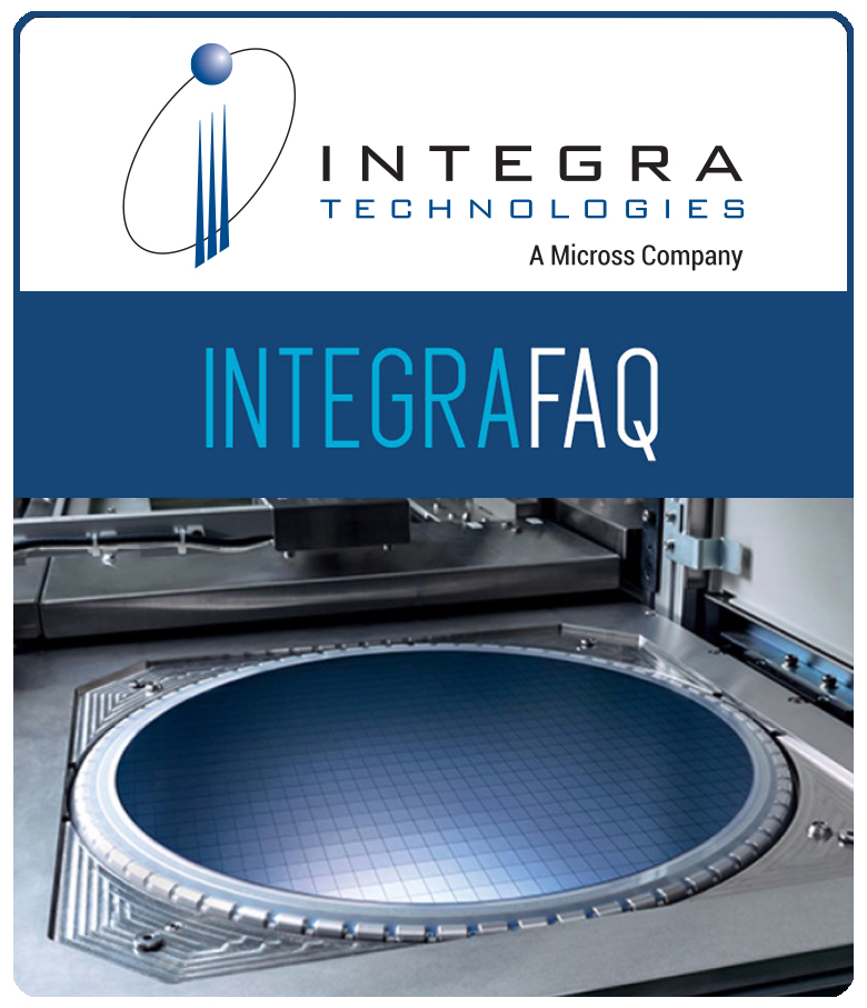
Integra Technologies - Dice Before Grind (DBG)
|
|
|
|
|
|
|
|
Reduce Stress and Cracking with the "Dice Before Grind" Method Dice Before Grind (DBG) is a wafer singulation method where the wafer is partially cut (diced) into individual chips before the wafer thinning (backgrinding) process. After dicing, a protective tape or material holds the die in place while the wafer is thinned down to its final thickness. The method is used to reduce stress and cracking compared to traditional “grind before dice” methods. It also allows handling of ultra-thin wafers that would otherwise be too fragile to dice after thinning. DBG also improves die strength and yield for advanced packaging applications like 3D ICs, SiP, and mobile devices. For more information, read Integra's September FAQ Newsletter! Integra is a Micross Company.
|
|
|
|
|
|
SemiDice - Supplier Spotlight
|
|
|
|
|
|
|
|
Featured Product CPM4-0230-0255ES0A
2300 V, 30 mΩ, Gen 4, Industrial qualified, Bare Die SiC MOSFET This is Wolfspeed’s 4th generation high-performance silicon carbide MOSFET, in a package-less bare die format to be implemented into any custom module design. The high blocking voltage with low on-resistance, and high-speed switching with low capacitance, makes this MOSFET ideal for high frequency switching applications including solar inverters and uninterrupted power supplies. SemiDice is a Micross Company.
|
|
|
|
|
|
|
|
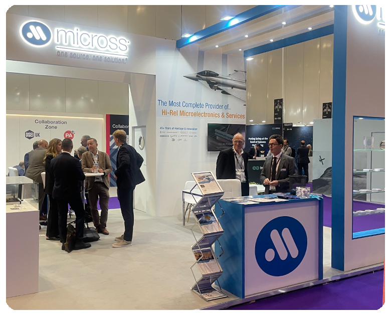
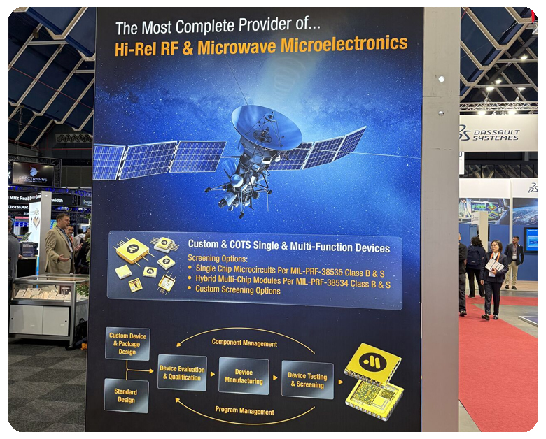
Micross will be showcasing our latest solutions for space, aerospace, defense, RF, and other hi-rel markets. Our product experts and executives will be on site to discuss your technical and program needs.
|
|
|
|
|
|
|
|
|
|
ISTFA - International Symposium for Testing and Failure Analysis November 16-20 Pasadena, CA Integra Technologies Booth #312
|
|
|
|
|
|
|
|
Space Tech Expo Europe November 18-20 Bremen, Germany Booth C40
|
|
|
|
|
|
|
|
|
|
EUMW - European Microwave Week
|
|
|
|
|